Introduction
Semiconductor Yield Management Software helps semiconductor manufacturers, foundries, chip designers, and electronics companies monitor, analyze, optimize, and improve manufacturing yield across wafer fabrication, packaging, testing, and production workflows. These platforms provide advanced analytics, defect detection, process monitoring, AI-driven root cause analysis, statistical process control, and manufacturing intelligence to maximize chip production efficiency and reduce costly defects.
As semiconductor manufacturing becomes increasingly complex with smaller process nodes, advanced packaging, AI chips, and high-volume production demands, traditional manual analysis methods are no longer sufficient. Modern yield management platforms now combine AI-driven analytics, machine learning, digital twins, real-time equipment monitoring, predictive maintenance, cloud-native collaboration, and advanced visualization workflows to improve production quality and operational efficiency.
Real-world use cases include:
- Wafer defect detection and classification
- Semiconductor process optimization
- Root cause analysis for yield loss
- Statistical process control and monitoring
- Advanced packaging and test analytics
Buyers evaluating Semiconductor Yield Management Software should focus on:
- AI-driven defect analysis capabilities
- Statistical process control functionality
- Real-time manufacturing analytics support
- Integration with fab equipment and MES systems
- Predictive maintenance and anomaly detection
- Cloud scalability and operational visibility
- Advanced visualization and reporting tools
- Security and IP protection capabilities
- Support for advanced process nodes
- Integration with inspection and metrology systems
Best for: Semiconductor foundries, chip manufacturers, electronics companies, advanced packaging facilities, wafer fabs, and enterprise semiconductor operations managing high-volume chip production environments.
Not ideal for: Small electronics labs or organizations requiring only lightweight manufacturing reporting without advanced yield analytics, process control, or semiconductor-specific manufacturing intelligence.
Key Trends in Semiconductor Yield Management Software
- AI-driven defect classification improving manufacturing yield
- Machine learning accelerating root cause analysis
- Real-time fab analytics replacing delayed reporting workflows
- Digital twins improving semiconductor manufacturing intelligence
- Cloud-native manufacturing visibility increasing globally
- Predictive maintenance reducing equipment downtime
- Advanced packaging analytics becoming critical
- High-performance data processing expanding rapidly
- Automated anomaly detection reducing manual inspections
- Cybersecurity becoming essential for semiconductor IP protection
How We Selected These Tools (Methodology)
- Adoption across semiconductor manufacturing environments
- Yield analytics and defect management depth
- AI and machine learning capabilities
- Integration with MES, metrology, and inspection systems
- Scalability for enterprise fab operations
- Security and governance capabilities
- Cloud deployment and operational visibility support
- Reporting and visualization functionality
- Predictive analytics and anomaly detection support
- Balance between enterprise, semiconductor-focused, and AI-driven solutions
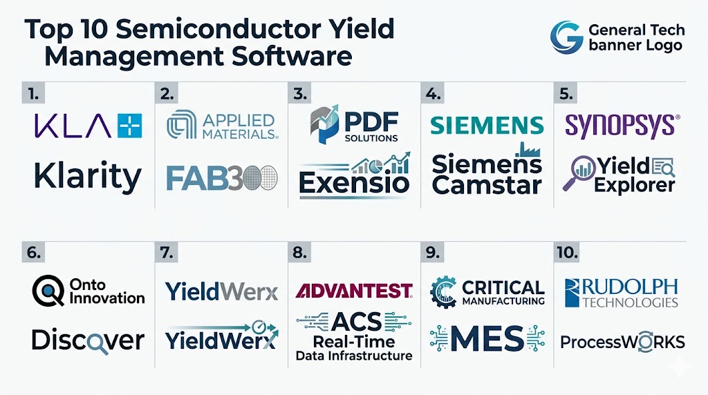
Top 10 Semiconductor Yield Management Software
1- PDF Solutions Exensio
Short description:
PDF Solutions Exensio is one of the most widely used semiconductor yield management platforms designed for advanced analytics, process optimization, and AI-driven manufacturing intelligence.
Key Features
- Yield analytics and monitoring
- AI-driven root cause analysis
- Statistical process control workflows
- Defect classification support
- Real-time fab dashboards
- Predictive maintenance analytics
- Semiconductor manufacturing intelligence
Pros
- Strong semiconductor-specific analytics
- Excellent AI-driven yield optimization
- Reliable enterprise scalability
Cons
- Premium enterprise pricing
- Complex deployment workflows
- Requires semiconductor process expertise
Platforms / Deployment
- Web
- Cloud / Hybrid
Security & Compliance
Supports RBAC, MFA, encryption, audit logging, and governance workflows.
Integrations & Ecosystem
Integrates with MES platforms, metrology tools, inspection systems, fab equipment, and analytics environments.
- APIs
- MES systems
- Metrology platforms
- Inspection tools
- Fab equipment
Support & Community
Large semiconductor manufacturing ecosystem.
2- KLA Klarity Analytics
Short description:
KLA Klarity Analytics provides defect analytics, yield optimization, and advanced process monitoring workflows for semiconductor manufacturing environments.
Key Features
- Defect classification analytics
- Yield monitoring workflows
- Process control dashboards
- AI-assisted anomaly detection
- Fab equipment monitoring
- Statistical analysis tools
- Root cause analysis support
Pros
- Strong inspection and metrology integration
- Excellent defect analytics capabilities
- Reliable fab operational visibility
Cons
- Enterprise deployment complexity
- Premium licensing structure
- Best optimized within KLA ecosystems
Platforms / Deployment
- Web
- Cloud / Hybrid
Security & Compliance
Supports secure authentication, encryption, RBAC, and governance controls.
Integrations & Ecosystem
- KLA inspection tools
- APIs
- MES systems
- Fab analytics platforms
Support & Community
Strong semiconductor process ecosystem.
3- Applied Materials FAB300
Short description:
Applied Materials FAB300 provides semiconductor manufacturing execution, process monitoring, and yield optimization workflows for wafer fabrication environments.
Key Features
- Fab process monitoring
- Yield optimization analytics
- Equipment integration workflows
- Statistical process control
- Operational reporting dashboards
- Defect monitoring support
- Real-time manufacturing visibility
Pros
- Strong fab equipment integration
- Good manufacturing visibility
- Reliable semiconductor operational workflows
Cons
- Enterprise implementation complexity
- Premium industrial pricing
- Requires semiconductor manufacturing expertise
Platforms / Deployment
- Web / Windows
- Hybrid / Self-hosted
Security & Compliance
Supports secure APIs, encryption, RBAC, and governance workflows.
Integrations & Ecosystem
- Fab equipment
- MES systems
- APIs
- Manufacturing analytics tools
Support & Community
Large semiconductor manufacturing ecosystem.
4- Synopsys Yield Explorer
Short description:
Synopsys Yield Explorer provides yield analysis, design-for-manufacturability workflows, and semiconductor process optimization for chip manufacturing environments.
Key Features
- Yield analysis workflows
- DFM optimization support
- Semiconductor defect analytics
- Process monitoring dashboards
- AI-assisted yield forecasting
- Operational analytics support
- Design and manufacturing integration
Pros
- Strong design-to-manufacturing visibility
- Reliable semiconductor analytics
- Good predictive modeling support
Cons
- Requires advanced semiconductor expertise
- Enterprise deployment complexity
- Premium licensing costs
Platforms / Deployment
- Web / Linux
- Cloud / Hybrid
Security & Compliance
Supports encryption, RBAC, secure APIs, and governance workflows.
Integrations & Ecosystem
- EDA systems
- APIs
- MES platforms
- Manufacturing databases
Support & Community
Strong semiconductor design ecosystem.
5- Siemens Opcenter Semiconductor
Short description:
Siemens Opcenter Semiconductor provides manufacturing execution, yield analytics, and process optimization workflows for semiconductor production environments.
Key Features
- Semiconductor MES workflows
- Yield and process analytics
- Production monitoring dashboards
- Statistical process control
- Operational reporting support
- Equipment integration capabilities
- Quality management workflows
Pros
- Strong MES and manufacturing integration
- Reliable operational visibility
- Good enterprise scalability
Cons
- Enterprise deployment requirements
- Complex workflow configuration
- Premium implementation costs
Platforms / Deployment
- Web
- Cloud / Hybrid
Security & Compliance
Supports MFA, RBAC, encryption, and governance workflows.
Integrations & Ecosystem
- MES systems
- APIs
- Manufacturing equipment
- ERP platforms
Support & Community
Large industrial manufacturing ecosystem.
6- Onto Innovation Discover
Short description:
Onto Innovation Discover provides semiconductor process analytics, yield optimization, and defect management workflows for advanced semiconductor manufacturing.
Key Features
- Defect inspection analytics
- Yield optimization workflows
- AI-assisted process analysis
- Metrology integration support
- Operational dashboards
- Statistical process monitoring
- Advanced packaging analytics
Pros
- Strong advanced packaging workflows
- Good metrology integration support
- Reliable defect analysis capabilities
Cons
- Enterprise semiconductor complexity
- Premium industrial pricing
- Requires process engineering expertise
Platforms / Deployment
- Web
- Cloud / Hybrid
Security & Compliance
Supports secure operational workflows and governance controls.
Integrations & Ecosystem
- Inspection systems
- APIs
- Metrology platforms
- Manufacturing analytics tools
Support & Community
Growing semiconductor process ecosystem.
7- CamLine LineWorks SPACE
Short description:
CamLine LineWorks SPACE provides semiconductor SPC, manufacturing analytics, and yield monitoring workflows for high-volume production environments.
Key Features
- Statistical process control workflows
- Semiconductor analytics dashboards
- Yield monitoring support
- Operational reporting tools
- AI-assisted anomaly detection
- Process optimization analytics
- Fab equipment integrations
Pros
- Strong SPC functionality
- Reliable semiconductor analytics
- Good operational visibility support
Cons
- Smaller ecosystem than major enterprise vendors
- Advanced customization may require expertise
- Enterprise deployment complexity
Platforms / Deployment
- Web
- Cloud / Hybrid
Security & Compliance
Supports secure authentication, encryption, and governance workflows.
Integrations & Ecosystem
- MES systems
- APIs
- Fab equipment
- Manufacturing reporting tools
Support & Community
Strong semiconductor operations ecosystem.
8- YieldWerx
Short description:
YieldWerx provides cloud-based semiconductor yield analytics and manufacturing intelligence workflows focused on fabless and semiconductor manufacturing environments.
Key Features
- Cloud-based yield analytics
- Defect and anomaly analysis
- Operational dashboards
- Process optimization workflows
- AI-assisted reporting support
- Manufacturing visibility tools
- Statistical analysis capabilities
Pros
- Strong cloud-native usability
- Easier deployment workflows
- Good fabless semiconductor support
Cons
- Smaller ecosystem than major enterprise platforms
- Limited advanced MES functionality
- Advanced customization capabilities vary
Platforms / Deployment
- Web
- Cloud
Security & Compliance
Supports encryption, RBAC, and governance workflows.
Integrations & Ecosystem
- APIs
- MES systems
- Manufacturing databases
- Analytics platforms
Support & Community
Growing semiconductor analytics ecosystem.
9- Critical Manufacturing MES
Short description:
Critical Manufacturing MES provides semiconductor-focused manufacturing execution, yield monitoring, and operational analytics workflows for smart factory environments.
Key Features
- Semiconductor MES workflows
- Yield and quality analytics
- Smart factory integration support
- Real-time operational dashboards
- AI-assisted process monitoring
- Equipment integration workflows
- Reporting and traceability support
Pros
- Strong smart manufacturing support
- Reliable semiconductor operational workflows
- Good scalability capabilities
Cons
- Enterprise implementation complexity
- Premium deployment costs
- Requires manufacturing operations expertise
Platforms / Deployment
- Web
- Cloud / Hybrid
Security & Compliance
Supports secure APIs, RBAC, encryption, and governance workflows.
Integrations & Ecosystem
- MES systems
- APIs
- Manufacturing equipment
- ERP platforms
Support & Community
Strong semiconductor manufacturing ecosystem.
10- ProteanTecs
Short description:
ProteanTecs provides AI-driven semiconductor monitoring, predictive analytics, and lifecycle intelligence workflows for advanced chip manufacturing environments.
Key Features
- AI-driven chip monitoring
- Predictive analytics workflows
- Real-time operational intelligence
- Yield optimization analytics
- Lifecycle monitoring support
- Defect prediction capabilities
- Manufacturing visibility dashboards
Pros
- Strong AI-driven semiconductor analytics
- Good predictive intelligence workflows
- Reliable lifecycle visibility support
Cons
- Advanced deployment complexity
- Premium enterprise pricing
- Requires advanced semiconductor expertise
Platforms / Deployment
- Web
- Cloud
Security & Compliance
Supports encryption, secure APIs, RBAC, and governance workflows.
Integrations & Ecosystem
- Semiconductor analytics tools
- APIs
- Manufacturing systems
- Lifecycle monitoring platforms
Support & Community
Growing semiconductor AI ecosystem.
Comparison Table
| Tool Name | Best For | Platforms Supported | Deployment | Standout Feature | Public Rating |
|---|---|---|---|---|---|
| PDF Solutions Exensio | Enterprise yield optimization | Web | Hybrid | AI-driven yield analytics | N/A |
| KLA Klarity Analytics | Defect analytics | Web | Hybrid | Inspection and metrology integration | N/A |
| Applied Materials FAB300 | Fab process monitoring | Web, Windows | Hybrid | Manufacturing visibility | N/A |
| Synopsys Yield Explorer | Design-for-manufacturability | Web, Linux | Hybrid | Design-to-manufacturing analytics | N/A |
| Siemens Opcenter Semiconductor | Semiconductor MES | Web | Hybrid | Integrated MES workflows | N/A |
| Onto Innovation Discover | Advanced packaging analytics | Web | Hybrid | Metrology-driven yield optimization | N/A |
| CamLine LineWorks SPACE | SPC and process analytics | Web | Hybrid | Statistical process control | N/A |
| YieldWerx | Cloud semiconductor analytics | Web | Cloud | Cloud-native yield visibility | N/A |
| Critical Manufacturing MES | Smart semiconductor factories | Web | Hybrid | Smart manufacturing workflows | N/A |
| ProteanTecs | AI semiconductor intelligence | Web | Cloud | Predictive chip analytics | N/A |
Evaluation & Scoring of Semiconductor Yield Management Software
| Tool Name | Core 25% | Ease 15% | Integrations 15% | Security 10% | Performance 10% | Support 10% | Value 15% | Weighted Total |
|---|---|---|---|---|---|---|---|---|
| PDF Solutions Exensio | 9.6 | 8.0 | 9.3 | 9.2 | 9.5 | 9.2 | 8.0 | 9.1 |
| KLA Klarity Analytics | 9.4 | 7.8 | 9.4 | 9.1 | 9.4 | 9.1 | 7.9 | 8.9 |
| Applied Materials FAB300 | 9.1 | 7.7 | 9.1 | 9.0 | 9.2 | 9.0 | 8.0 | 8.7 |
| Synopsys Yield Explorer | 9.2 | 7.8 | 9.2 | 9.0 | 9.1 | 9.0 | 8.0 | 8.8 |
| Siemens Opcenter Semiconductor | 9.0 | 7.9 | 9.1 | 9.1 | 9.0 | 9.0 | 8.1 | 8.7 |
| Onto Innovation Discover | 8.9 | 7.9 | 8.9 | 8.9 | 8.9 | 8.8 | 8.2 | 8.6 |
| CamLine LineWorks SPACE | 8.8 | 8.1 | 8.7 | 8.8 | 8.8 | 8.7 | 8.4 | 8.6 |
| YieldWerx | 8.7 | 8.5 | 8.5 | 8.7 | 8.7 | 8.5 | 8.8 | 8.6 |
| Critical Manufacturing MES | 8.9 | 8.0 | 8.9 | 9.0 | 8.9 | 8.8 | 8.3 | 8.7 |
| ProteanTecs | 9.1 | 7.9 | 8.8 | 9.0 | 9.1 | 8.8 | 8.2 | 8.7 |
These scores are comparative and intended to help organizations evaluate Semiconductor Yield Management Software based on analytics depth, AI capabilities, integrations, scalability, operational visibility, cybersecurity, and long-term semiconductor manufacturing value.
Which Semiconductor Yield Management Software Is Right for You?
Small Semiconductor Design Teams
Best suited: YieldWerx, CamLine LineWorks SPACE
These provide easier deployment and strong analytics workflows for smaller operations.
SMB Semiconductor Manufacturers
Best suited: Onto Innovation Discover, Critical Manufacturing MES
These balance operational visibility and semiconductor manufacturing intelligence.
Mid-Market Semiconductor Operations
Best suited: Siemens Opcenter Semiconductor, Synopsys Yield Explorer
These provide stronger process optimization and manufacturing analytics capabilities.
Large Enterprise Foundries and Chip Manufacturers
Best suited: PDF Solutions Exensio, KLA Klarity Analytics, Applied Materials FAB300
These offer enterprise scalability, advanced defect analytics, and deep semiconductor manufacturing intelligence.
Budget vs Premium
Budget-friendly: YieldWerx, CamLine LineWorks SPACE
Premium enterprise: PDF Solutions Exensio, KLA Klarity Analytics
Feature Depth vs Ease of Use
Deep enterprise functionality: PDF Solutions Exensio, Synopsys Yield Explorer
Ease of use: YieldWerx, CamLine LineWorks SPACE
Integrations & Scalability
Best integrations: KLA Klarity Analytics, Siemens Opcenter Semiconductor, Applied Materials FAB300
Best scalability: PDF Solutions Exensio, KLA Klarity Analytics
Security & Compliance Needs
Semiconductor manufacturers managing sensitive IP and advanced manufacturing operations should prioritize systems supporting RBAC, MFA, encryption, audit logging, and secure fab operational workflows.
Frequently Asked Questions
1. What is Semiconductor Yield Management Software?
It is software used to monitor, analyze, optimize, and improve semiconductor manufacturing yield and process quality.
2. Why is yield management important in semiconductor manufacturing?
It helps reduce defects, improve production efficiency, increase profitability, and optimize advanced manufacturing workflows.
3. Can these platforms integrate with fab equipment?
Yes, most modern semiconductor yield management platforms integrate deeply with MES systems, inspection tools, metrology platforms, and fab equipment.
4. What analytics capabilities are common?
Defect classification, root cause analysis, predictive maintenance, anomaly detection, SPC, and AI-driven process optimization are commonly supported.
5. Are cloud-based semiconductor analytics platforms common?
Yes, cloud-native semiconductor analytics platforms are increasingly common because they improve scalability and operational visibility.
6. What security features are important?
RBAC, MFA, encryption, secure APIs, and audit logging are critical for protecting semiconductor manufacturing IP and operational data.
7. Which industries use semiconductor yield management software most?
Semiconductor foundries, chip manufacturers, electronics companies, and advanced packaging facilities heavily rely on these platforms.
8. Can these platforms support AI-driven analytics?
Yes, many modern platforms now include AI-assisted defect detection, predictive analytics, and automated process optimization workflows.
9. What are common implementation challenges?
MES integration, data normalization, user training, fab equipment connectivity, and workflow customization are common deployment challenges.
10. How should organizations choose a semiconductor yield management platform?
Organizations should evaluate analytics depth, integrations, AI capabilities, scalability, cybersecurity, and long-term manufacturing strategy.
Conclusion
Semiconductor Yield Management Software has become essential infrastructure for organizations managing increasingly advanced semiconductor manufacturing environments and process complexities. Modern platforms now combine AI-driven analytics, predictive maintenance, defect classification, digital twins, cloud collaboration, and real-time manufacturing visibility to support intelligent semiconductor production operations. Enterprise solutions such as PDF Solutions Exensio, KLA Klarity Analytics, and Applied Materials FAB300 provide deep operational functionality and advanced yield intelligence, while platforms like YieldWerx and CamLine LineWorks SPACE offer flexible and accessible workflows for evolving semiconductor environments. The best solution ultimately depends on manufacturing scale, process complexity, integration priorities, AI requirements, and long-term semiconductor strategy. A structured evaluation process combined with pilot deployments and workflow validation can significantly improve production yield, operational efficiency, and long-term semiconductor manufacturing performance.