Introduction
PCB (Printed Circuit Board) design software is a specialized category of Electronic Design Automation (EDA) tools used to design, simulate, and prepare circuit boards for manufacturing. These tools allow engineers to create schematics, route electrical connections, validate designs, and generate manufacturing files such as Gerber outputs.
As electronic devices become more compact and complex, PCB design software has become essential for ensuring signal integrity, power efficiency, and manufacturability. From consumer electronics to industrial systems, these tools enable faster iteration and higher reliability.
Common use cases include:
- Designing multi-layer PCBs for electronics
- Schematic capture and circuit simulation
- Signal integrity and power analysis
- Generating manufacturing-ready files
- Prototyping and product development
Key evaluation criteria:
- Schematic and layout capabilities
- Routing automation and design rule checks
- Component libraries and sourcing integration
- Simulation and validation features
- Ease of use and learning curve
- Collaboration and version control
- Manufacturing integration (DFM, Gerber output)
- Performance with complex boards
- Pricing and licensing flexibility
Best for: Electronics engineers, PCB designers, embedded engineers, hardware startups, and manufacturing teams.
Not ideal for: Users who only need basic circuit diagrams or non-manufacturable designs—simpler schematic tools may suffice.
Key Trends in PCB Design Software
- AI-assisted routing: Tools now suggest optimal routing paths and component placement
- Cloud-based PCB design: Increasing use of browser-based tools for collaboration
- Real-time design rule checking (DRC): Faster validation during design workflows
- Integrated supply chain data: Real-time component availability and sourcing insights
- Multi-board and system-level design: Managing complex electronic systems
- 3D visualization and MCAD integration: Better alignment with mechanical design
- Open-source ecosystem growth: Tools like KiCad gaining strong adoption
- Simulation-first workflows: Integrated SPICE and signal integrity analysis
- Subscription licensing models: Flexible pricing replacing perpetual licenses
- Design for manufacturability (DFM): Built-in checks to reduce production errors
How We Selected These Tools (Methodology)
- Evaluated industry adoption and reputation
- Assessed core PCB design capabilities (schematic + layout)
- Reviewed routing, simulation, and validation features
- Analyzed integration with manufacturing workflows
- Considered ease of use for beginners and professionals
- Evaluated cloud vs desktop deployment flexibility
- Reviewed component libraries and ecosystem strength
- Considered support, documentation, and training resources
- Included both enterprise and open-source tools
- Ensured coverage across different user segments
Top 10 PCB Design Software Tools
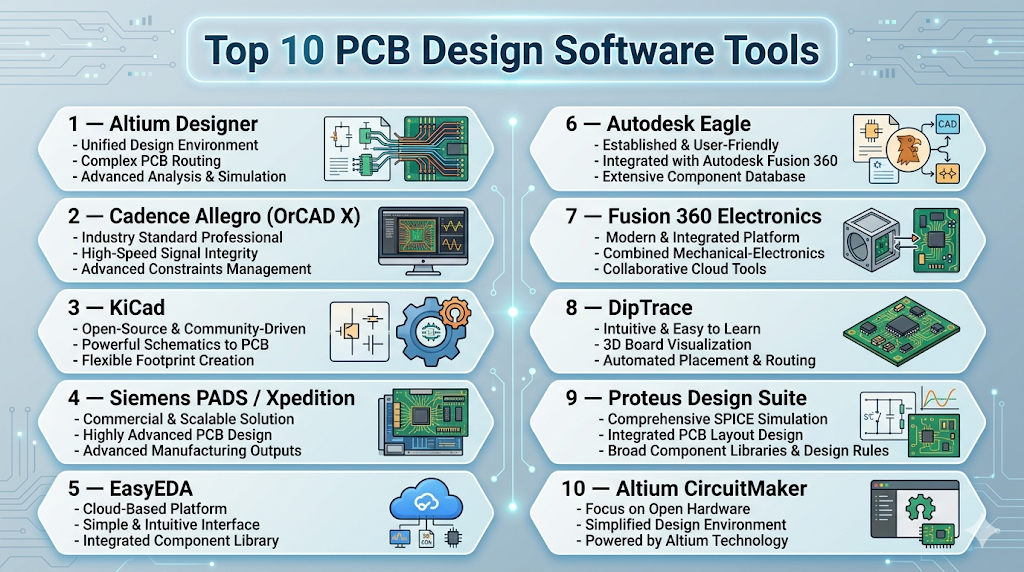
#1 — Altium Designer
Short description: A professional-grade PCB design platform widely used for complex, high-speed electronic systems.
Key Features
- Unified schematic and PCB design environment
- Advanced routing and constraint management
- Signal integrity analysis
- 3D PCB visualization
- Integrated component sourcing
- Real-time collaboration tools
Pros
- Comprehensive all-in-one platform
- Industry-standard for professional design
Cons
- Expensive
- Learning curve for beginners
Platforms / Deployment
- Windows
- Cloud / Self-hosted
Security & Compliance
- Not publicly stated
Integrations & Ecosystem
Strong ecosystem for professional workflows.
- Component libraries
- MCAD integration
- Cloud collaboration
- APIs
Support & Community
Extensive documentation and large professional community.
#2 — Cadence Allegro (OrCAD X)
Short description: A powerful PCB design suite for enterprise and mid-market engineering teams.
Key Features
- Advanced PCB layout and routing
- Real-time design rule checking
- SPICE simulation
- High-speed design support
- Cloud-connected workflows
Pros
- Strong performance for complex boards
- Scalable for enterprise use
Cons
- Steep learning curve
- Expensive
Platforms / Deployment
- Windows
- Cloud / Self-hosted
Security & Compliance
- Not publicly stated
Integrations & Ecosystem
Integrated with broader Cadence ecosystem.
- Simulation tools
- Manufacturing workflows
- APIs
Support & Community
Strong enterprise support.
#3 — KiCad
Short description: A leading open-source PCB design tool offering professional capabilities without licensing costs.
Key Features
- Schematic capture and PCB layout
- SPICE simulation
- 3D visualization
- Gerber file generation
- BOM creation
- Multi-layer board support
Pros
- Free and open-source
- Cross-platform support
Cons
- UI inconsistencies
- Limited enterprise features
Platforms / Deployment
- Windows / macOS / Linux
- Self-hosted
Security & Compliance
- Not publicly stated
Integrations & Ecosystem
Extensible with plugins and community tools.
- Component libraries
- APIs
- Simulation tools
Support & Community
Large and active open-source community.
#4 — Siemens PADS / Xpedition
Short description: Enterprise-grade PCB design tools for large-scale and complex electronic systems.
Key Features
- Advanced PCB layout
- Signal integrity analysis
- Design rule checking
- Multi-board design
- Manufacturing integration
Pros
- Highly scalable
- Strong enterprise capabilities
Cons
- Expensive
- Complex interface
Platforms / Deployment
- Windows
- Self-hosted
Security & Compliance
- Not publicly stated
Integrations & Ecosystem
Supports enterprise workflows.
- CAD tools
- Manufacturing tools
- APIs
Support & Community
Strong enterprise support.
#5 — EasyEDA
Short description: A browser-based PCB design tool ideal for beginners and quick prototyping.
Key Features
- Web-based schematic capture
- PCB layout tools
- SPICE simulation
- Component libraries
- Manufacturing integration
Pros
- Easy to use
- No installation required
Cons
- Limited advanced features
- Internet dependency
Platforms / Deployment
- Web
- Cloud
Security & Compliance
- Not publicly stated
Integrations & Ecosystem
Cloud-focused design ecosystem.
- Component sourcing
- Manufacturing services
- APIs
Support & Community
Growing user base and tutorials.
#6 — Autodesk Eagle
Short description: A widely used PCB design tool known for accessibility and integration with design workflows.
Key Features
- Schematic capture
- PCB layout
- Component libraries
- Design rule checks
- Integration with CAD tools
Pros
- Easy to learn
- Good for small projects
Cons
- Limited advanced features
- Transition toward other platforms
Platforms / Deployment
- Windows / macOS
- Cloud / Self-hosted
Security & Compliance
- Not publicly stated
Integrations & Ecosystem
Part of a broader design ecosystem.
- CAD tools
- Cloud storage
- APIs
Support & Community
Strong community and documentation.
#7 — Fusion 360 Electronics
Short description: A unified platform combining PCB design with mechanical and manufacturing workflows.
Key Features
- Integrated PCB and mechanical design
- Cloud collaboration
- 3D modeling
- Simulation tools
- Manufacturing integration
Pros
- All-in-one platform
- Good for product teams
Cons
- Limited advanced PCB features
- Performance constraints
Platforms / Deployment
- Web / Windows / macOS
- Cloud
Security & Compliance
- Not publicly stated
Integrations & Ecosystem
Strong integration with design tools.
- CAD tools
- Cloud services
- APIs
Support & Community
Active community and documentation.
#8 — DipTrace
Short description: A cost-effective PCB design tool with strong usability and solid feature set.
Key Features
- Schematic capture
- PCB layout
- Autorouting
- 3D preview
- Multi-layer support
Pros
- Easy to learn
- Affordable
Cons
- Limited enterprise capabilities
- Smaller ecosystem
Platforms / Deployment
- Windows / macOS
- Self-hosted
Security & Compliance
- Not publicly stated
Integrations & Ecosystem
Supports standard workflows.
- Component libraries
- Export formats
- APIs
Support & Community
Moderate community support.
#9 — Proteus Design Suite
Short description: A simulation-focused PCB design tool widely used in education and embedded systems development.
Key Features
- Circuit simulation
- PCB layout
- Microcontroller simulation
- Debugging tools
- Component libraries
Pros
- Strong simulation capabilities
- Useful for embedded development
Cons
- Limited advanced PCB design features
- Interface complexity
Platforms / Deployment
- Windows
- Self-hosted
Security & Compliance
- Not publicly stated
Integrations & Ecosystem
Supports embedded workflows.
- Microcontroller tools
- Simulation libraries
- APIs
Support & Community
Popular in academic environments.
#10 — Altium CircuitMaker
Short description: A free PCB design tool aimed at makers and hobbyists with access to professional features.
Key Features
- Schematic capture
- PCB layout
- Community component libraries
- Collaboration tools
- Design sharing
Pros
- Free access
- Backed by professional ecosystem
Cons
- Limited compared to full Altium
- Requires online account
Platforms / Deployment
- Windows
- Cloud / Self-hosted
Security & Compliance
- Not publicly stated
Integrations & Ecosystem
Connected to Altium ecosystem.
- Component libraries
- Cloud sharing
- APIs
Support & Community
Active maker community.
Comparison Table (Top 10)
| Tool Name | Best For | Platform(s) Supported | Deployment | Standout Feature | Public Rating |
|---|---|---|---|---|---|
| Altium Designer | Professionals | Windows | Hybrid | Unified environment | N/A |
| Cadence Allegro | Enterprise | Windows | Hybrid | High-speed design | N/A |
| KiCad | Open-source users | All major OS | Self-hosted | Free & powerful | N/A |
| Siemens PADS | Large teams | Windows | Self-hosted | Scalability | N/A |
| EasyEDA | Beginners | Web | Cloud | Browser-based | N/A |
| Autodesk Eagle | Small projects | Windows, macOS | Hybrid | Accessibility | N/A |
| Fusion 360 Electronics | Product teams | Web, Desktop | Cloud | Integrated design | N/A |
| DipTrace | SMB | Windows, macOS | Self-hosted | Ease of use | N/A |
| Proteus | Education | Windows | Self-hosted | Simulation | N/A |
| CircuitMaker | Hobbyists | Windows | Hybrid | Free ecosystem | N/A |
Evaluation & Scoring of PCB Design Software
| Tool Name | Core (25%) | Ease (15%) | Integrations (15%) | Security (10%) | Performance (10%) | Support (10%) | Value (15%) | Weighted Total (0–10) |
|---|---|---|---|---|---|---|---|---|
| Altium | 10 | 7 | 9 | 7 | 9 | 9 | 6 | 8.5 |
| Cadence | 10 | 6 | 9 | 7 | 10 | 9 | 6 | 8.6 |
| KiCad | 8 | 8 | 7 | 5 | 8 | 8 | 10 | 7.9 |
| Siemens | 9 | 6 | 8 | 7 | 9 | 8 | 6 | 8.0 |
| EasyEDA | 7 | 9 | 7 | 5 | 7 | 7 | 9 | 7.6 |
| Eagle | 7 | 8 | 7 | 6 | 7 | 7 | 8 | 7.3 |
| Fusion 360 | 7 | 9 | 7 | 6 | 7 | 8 | 9 | 7.8 |
| DipTrace | 7 | 8 | 6 | 5 | 7 | 7 | 8 | 7.2 |
| Proteus | 7 | 7 | 6 | 5 | 7 | 7 | 7 | 6.9 |
| CircuitMaker | 6 | 8 | 7 | 5 | 6 | 7 | 9 | 7.0 |
How to interpret scores:
- Enterprise tools dominate in performance and advanced capabilities
- Open-source tools offer strong value with moderate trade-offs
- Cloud tools excel in usability and collaboration
- Ease of use often comes at the cost of advanced features
- Always prioritize your workflow needs over total score
Which PCB Design Software Tool Is Right for You?
Solo / Freelancer
- Best options: KiCad, EasyEDA, CircuitMaker
- Focus on cost-effectiveness and ease of use
SMB
- Best options: DipTrace, Fusion 360 Electronics, Eagle
- Balance between affordability and capability
Mid-Market
- Best options: Altium Designer, OrCAD
- Need advanced features with manageable complexity
Enterprise
- Best options: Cadence Allegro, Siemens Xpedition
- High-performance and large-scale design
Budget vs Premium
- Budget: KiCad, EasyEDA
- Premium: Altium, Cadence
Feature Depth vs Ease of Use
- Easy: EasyEDA, DipTrace
- Advanced: Cadence, Altium
Integrations & Scalability
- Strong: Cadence, Siemens
- Moderate: Fusion 360
Security & Compliance Needs
- Enterprise tools offer better governance
- Cloud tools require evaluation of data handling
Frequently Asked Questions (FAQs)
What is PCB design software used for?
It is used to design circuit boards, simulate performance, and generate manufacturing files.
Is PCB design software expensive?
It ranges from free open-source tools to high-cost enterprise platforms.
Which tool is best for beginners?
EasyEDA and KiCad are popular beginner-friendly options.
Can I design PCBs online?
Yes, cloud-based tools allow browser-based design.
What files are generated for manufacturing?
Gerber files, BOM, and drill files are commonly generated.
Do I need simulation features?
Simulation helps validate designs before production but is optional.
Can open-source tools be used professionally?
Yes, tools like KiCad are widely used in professional environments.
How long does it take to learn PCB design?
Basic skills can be learned quickly, but advanced expertise takes time.
What industries use PCB software?
Consumer electronics, automotive, aerospace, and industrial systems.
Is collaboration supported?
Many modern tools support real-time collaboration and version control.
Conclusion
PCB design software is a critical part of modern electronics development, enabling engineers to design, test, and manufacture complex circuit boards efficiently. From enterprise solutions like Cadence and Altium to accessible tools like KiCad and EasyEDA, the ecosystem provides options for every skill level and budget.